Sofort lieferbar (Download)
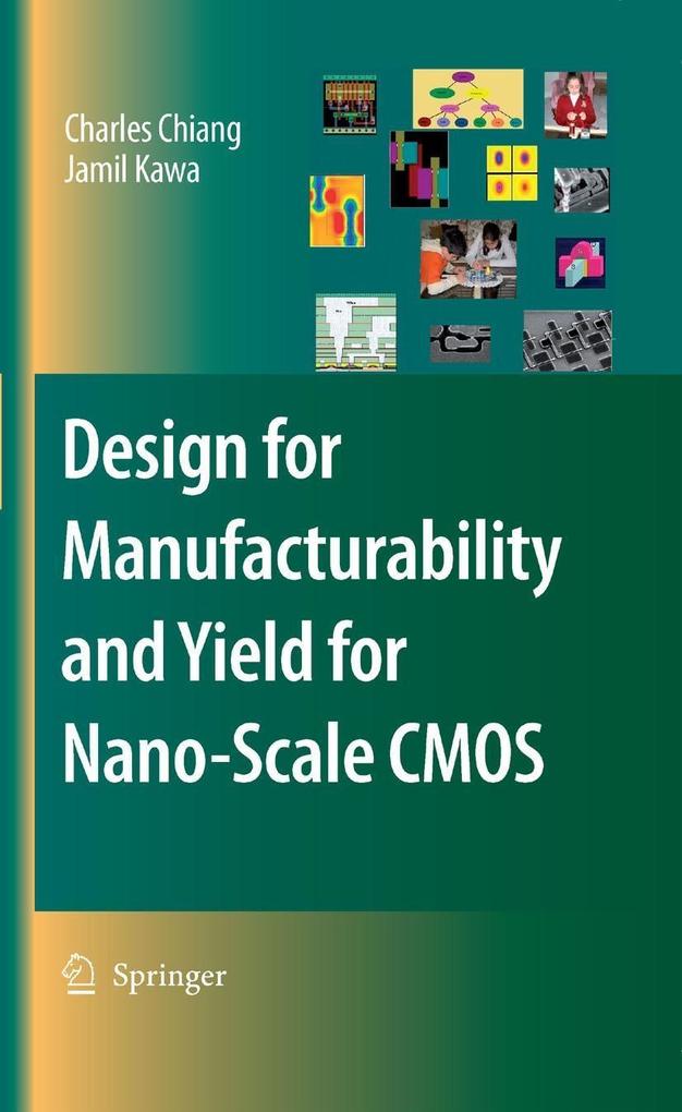
As we approach the 32 nm CMOS technology node the design and manufacturing communities are dealing with a lithography system that has to print circuit artifacts that are significantly less than half the wavelength of the light source used, with new materials, with tighter pitches, and higher aspect ratio metallurgies. This reality has resulted in three main manufacturability issues that have to be addressed: printability, planarization, and intra-die variability. Addressing in depth the fundamentals impacting those three issues at all the stages of the design process is not a luxury one can ignore. Manufacturability and yield are now one and the same and are no longer a fabrication, packaging, and test concerns; they are the concern of the whole IC community. Yield and manufacturability have to be designed in, and they are everybody's responsibility.
Design for Manufacturability and Yield for Nano-Scale CMOS walks the reader through all the aspects of manufacturability and yield in a nano-CMOS process and how to address each aspect at the proper design step starting with the design and layout of standard cells and how to yield-grade libraries for critical area and lithography artifacts through place and route, CMP model based simulation and dummy-fill insertion, mask planning, simulation and manufacturing, and through statistical design and statistical timing closure of the design. It alerts the designer to the pitfalls to watch for and to the good practices that can enhance a design's manufacturability and yield. This book is a must read book the serious practicing IC designer and an excellent primer for any graduate student intent on having a career in IC design or in EDA tool development.
Inhaltsverzeichnis
Random Defects. - Systematic Yield - Lithography. - Systematic Yield - Chemical Mechanical Polishing (CMP). - Variability & Parametric Yield. - Design for Yield. - Yield Prediction. - Conclusions.
Produktdetails
Erscheinungsdatum
15. Juni 2007
Sprache
englisch
Seitenanzahl
255
Dateigröße
41,39 MB
Reihe
Integrated Circuits and Systems
Autor/Autorin
Charles Chiang, Jamil Kawa
Verlag/Hersteller
Kopierschutz
mit Wasserzeichen versehen
Produktart
EBOOK
Dateiformat
PDF
ISBN
9781402051883
Entdecken Sie mehr
Bewertungen
0 Bewertungen
Es wurden noch keine Bewertungen abgegeben. Schreiben Sie die erste Bewertung zu "Design for Manufacturability and Yield for Nano-Scale CMOS" und helfen Sie damit anderen bei der Kaufentscheidung.


